Showing posts with label supply. Show all posts
Showing posts with label supply. Show all posts
Wednesday, December 18, 2013
Build a high volt supply Circuit Diagram
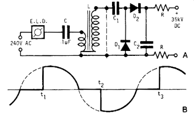
A light dimmer, a 1 µf capacitor and a 12 V car ignition coil form the simple line powered HV generator. The current in the dimmer is shown in Fig. B. At times tp t2, set by the dimmer switch, the inner triac of the dimmer switches on, and a very high and very fast current pulse charges the capacitor through the primary of the induction coil.
Then at a rate of 120 times per second for a 60 Hz line, a very high voltage pulse appears at the secondary of the coil. To obtain an HV dc output, use a voltage doubler. Dl and D2 are selenium rectifiers (TV 18 Siemens or ITT) used for the supply of television sets. High value output shock protection resistors, R, are recommended when suitable.
Build a high-volt supply Circuit Diagram

Thursday, July 25, 2013
Mains Supply Failure Alarm
Whenever AC mains supply fails, this circuit alerts you by sounding an alarm. It also provides a backup light to help you find your way to the torch or the generator key in the dark. The circuit is powered directly by a 9V PP3/6F22 compact battery. Pressing of switch S1 provides the 9V power supply to the circuit. A red LED (LED2), in conjunction with zener diode ZD1 (6V), is used to indicate the battery power level.
Resistor R9 limits the operating current (and hence the brightness) of LED2. When the battery voltage is 9V, LED2 glows with full intensity. As the battery voltage goes below 8V, the intensity of LED2 decreases and it glows very dimly. LED2 goes off when the battery voltage goes below 7.5V. Initially, in standby state, both the LEDs are off and the buzzer does not sound. The 230V AC mains is directly fed to mains-voltage detection optocoupler IC MCT2E (IC1) via resistors R1, R2 and R3, bridge rectifier BR1 and capacitor C1.
Illumination of the LED inside optocoupler IC1 activates its internal phototransistor and clock input pin 12 of IC2 (connected to 9V via N/C contact of relay RL1) is pulled low. Note that only one monostable of dual-monostable multivibrator IC CD4538 (IC2) is used here. When mains goes off, IC2 is triggered after a short duration determined by components C1, R4 and C3. Output pin 10 of IC2 goes high to forward bias relay driver transistor T1 via resistor R7.
Circuit diagram:
Resistor R9 limits the operating current (and hence the brightness) of LED2. When the battery voltage is 9V, LED2 glows with full intensity. As the battery voltage goes below 8V, the intensity of LED2 decreases and it glows very dimly. LED2 goes off when the battery voltage goes below 7.5V. Initially, in standby state, both the LEDs are off and the buzzer does not sound. The 230V AC mains is directly fed to mains-voltage detection optocoupler IC MCT2E (IC1) via resistors R1, R2 and R3, bridge rectifier BR1 and capacitor C1.
Illumination of the LED inside optocoupler IC1 activates its internal phototransistor and clock input pin 12 of IC2 (connected to 9V via N/C contact of relay RL1) is pulled low. Note that only one monostable of dual-monostable multivibrator IC CD4538 (IC2) is used here. When mains goes off, IC2 is triggered after a short duration determined by components C1, R4 and C3. Output pin 10 of IC2 goes high to forward bias relay driver transistor T1 via resistor R7.
Circuit diagram:

Mains Supply Failure Alarm Circuit Diagram
Relay RL1 energises to activate the piezo buzzer via its N/O contact for the time-out period of the monostable multivibrator (approximately 17 minutes). At the same time, the N/C contact removes the positive supply to resistor R4. The time-out period of the monostable multivibrator is determined by R5 and C2. Simultaneously, output pin 9 of IC2 goes low and pnp transistor T2 gets forward biased to light up the white LED (LED1).
Light provided by this back-up LED is sufficient to search the torch or generator key. During the mono time-out period, the circuit can be switched off by opening switch S1. The ‘on’ period of the monostable multivibrator may be changed by changing the value of resistor R5 or capacitor C2. If mains doesn’t resume when the ‘on’ period of the monostable lapses, the timer is retriggered after a short delay determined by resistor R4 and C3.
Light provided by this back-up LED is sufficient to search the torch or generator key. During the mono time-out period, the circuit can be switched off by opening switch S1. The ‘on’ period of the monostable multivibrator may be changed by changing the value of resistor R5 or capacitor C2. If mains doesn’t resume when the ‘on’ period of the monostable lapses, the timer is retriggered after a short delay determined by resistor R4 and C3.
Source: EFY Mag
Saturday, July 6, 2013
Simple Mini Bench Supply
Every electronics engineer is familiar with the anxiety of the moment when power is first applied to a newly-built circuit, wondering whether hours of work are about to be destroyed in a puff of smoke. A high-quality power supply with an adjustable current limit function is an excellent aid to steadying the nerves. Unfortunately power supplies with good regulation performance are expensive and homebrew construction is not always straightforward. Many of the ‘laboratory power supplies’ currently on the market are low-cost units based on switching regulators which, although certainly capable of delivering high currents, have rather poor ripple performance. Large output capacitors (which, in the case of a fault, will discharge into your circuit) and voltage over-shoot are other problems.
The power supply described here is a simple unit, easily constructed from standard components. It is only suitable for small loads but otherwise has all the characteristics of its bigger brethren. Between 18 V and 24 V is applied to the input, for example from a laptop power supply. This avoids the need for an expensive transformer and accompanying smoothing. No negative supply is needed, but the output voltage is nevertheless adjustable down to 0 V.
A difficulty in the design of power supplies with current limiting is the shunt resistor needed to measure the output current, normally connected to a differential amplifier. Frequently in simple designs the amplifier is not powered from a regulated supply, which can lead to an unstable current regulation loop. This circuit avoids the difficulty by using a low-cost fixed voltage regulator to supply the feedback circuit with a stable voltage. This arrangement greatly simplifies current measurement and regulation.
Mini Bench Supply Circuit Diagram

To generate this intermediate supply volt-age we use an LM7815. Its output passes through R17, which measures the output current, to MOSFET T1 which is driven by the voltage regulation opamp IC1C. Here R11 and C4 determine the bandwidth of the control loop, preventing oscillation at high frequencies. R15 ensures that capacitive loads with low effective resistance do not make the control loop unstable.
The negative feedback of AC components of the current via R12 and C5 makes the circuit reliable even with a large capacitor at its output, and negative feedback of the DC component is via the low-pass filter formed by R14 and C6. This ensures that the volt-age drop across R15 is correctly compensated for. C7 at the output provides a low impedance source for high-frequency loads, and R16 provides for the discharge of C17 when the set voltage is reduced with no load attached.
Current regulation is carried out by IC1D. Again to ensure stability, the bandwidth of the feedback loop is restricted by R19 and C8. If the voltage dropped across R17 exceeds the value set by P2, the current limit function comes into action and T2 begins to conduct. This in turn reduces the input voltage to the voltage regulation circuit until the desired current is reached. R7, R9 and C3 ensure that current regulation does not lead to output voltage over-shoots and that resonance does not occur with inductive loads.
The controls of the power supply are all voltage-based. This means, for example¸ that P1 and P2 can be replaced by digital-to-analogue converters or digital potentiometers so that the whole unit can be driven by a microcontroller. IC1B acts as a buffer to ensure that the dynamic characteristics of the circuit are not affected by the setting of P1. IC1A is used as a comparator whose out-put is used to drive two LEDs that indicate whether the supply is in voltage regulation or current regulation mode. If D2 lights the supply is in constant voltage mode; if D1 lights it is in constant current mode, for example if the output has been short-circuited. The power supply thus boasts all the features of a top-class bench supply.IC1A and its surrounding circuitry can be dispensed with if the mode indication is not wanted.
A type LM324 operational amplifier is suggested as, in contrast to many other similar devices, it operates reliably with input voltages down to 0 V. Other rail-to-rail opamps could equally well be used. The particular n-channel MOSFET devices used are not critical: a BUZ21, IRF540, IRF542 or 2SK1428 could be used for T1, for example, and a BS170 could be used in place of the 2N7002. The capacitors should all be rated for a voltage of 35 V or higher, and R15 and R17 must be at least 0.5 W types. The fixed voltage regulator and T1 must both be equipped with an adequate heatsink. If they are mounted on the same heatsink, they must be isolated from it as the tabs of the two devices are at different potentials.
Author : Alexander Mumm - Copyright : Elektor
Wednesday, July 3, 2013
Auto Changeover from Generator to Mains Supply
Because of energy crisis Load shedding may be a common problem in several countries.. Sudden power fluctuations, surge and high voltage may spoil sophisticated household appliances like TV, VCR, VCP and music system. This circuit provides protection against these problems and automatically changes the power supply from Generator output to mains supply and also switches off the generator.
Circuit descriptions
This circuit is self explanatory. When lines supply voltage crosses the preset level, Zener diode ZD4 break down and thus transistor T2 conducts, T3 does not conduct, causing the relay to de-energise. Voltage surge at the time of power resumption is protected by the delay circuit around transistor T1.
All the portable petrol and kerosene generators have a connection from CDI. To stop the engine of the generator-set, this connection is to be grounded momentarily (through the switch). This lead is to be connected with the ground through the N/C point of the relay.
Auto Changeover from Generator to Mains Supply Circuit Diagram

Instead of the one transformer, two transformers are used in series to ensure better life of the unit. Value of capacitor C2 can be increased or decreased for the variation of delay time. A negative feedback resistance, R6 (15 K-ohm to 100 k-ohm) can be incorporated between transistor T3 and T4 to overcome the damage that could be caused by voltage fluctuations.
Parts List:
Resistors (all ¼-watt, ± 5% Carbon)
R1 = 10 Ω
R2 = 1 KΩ
R3 = 820 Ω
R4 = 57 KΩ
R5 = 47 Ω
R6 = (15 KΩ to 100 KΩ)
Capacitors
C1 = 100 µF/25V
C2 = 1000 µF/12V
C3 = 100 µF/18V
Semiconductors
T1 = BC147
T2, T3 = SL100
D1, D2 = 1N4001
D3 = 1N4007
ZD1 = 5.6V/400mW
ZD2 = 7.8V/400mW
Miscellaneous
X1, X2 = 230V AC primary to 12 V, 500mA secondary transformers
RL1 = 12V/450 Ω relay
Circuit descriptions
This circuit is self explanatory. When lines supply voltage crosses the preset level, Zener diode ZD4 break down and thus transistor T2 conducts, T3 does not conduct, causing the relay to de-energise. Voltage surge at the time of power resumption is protected by the delay circuit around transistor T1.
All the portable petrol and kerosene generators have a connection from CDI. To stop the engine of the generator-set, this connection is to be grounded momentarily (through the switch). This lead is to be connected with the ground through the N/C point of the relay.
Auto Changeover from Generator to Mains Supply Circuit Diagram
Instead of the one transformer, two transformers are used in series to ensure better life of the unit. Value of capacitor C2 can be increased or decreased for the variation of delay time. A negative feedback resistance, R6 (15 K-ohm to 100 k-ohm) can be incorporated between transistor T3 and T4 to overcome the damage that could be caused by voltage fluctuations.
Parts List:
Resistors (all ¼-watt, ± 5% Carbon)
R1 = 10 Ω
R2 = 1 KΩ
R3 = 820 Ω
R4 = 57 KΩ
R5 = 47 Ω
R6 = (15 KΩ to 100 KΩ)
Capacitors
C1 = 100 µF/25V
C2 = 1000 µF/12V
C3 = 100 µF/18V
Semiconductors
T1 = BC147
T2, T3 = SL100
D1, D2 = 1N4001
D3 = 1N4007
ZD1 = 5.6V/400mW
ZD2 = 7.8V/400mW
Miscellaneous
X1, X2 = 230V AC primary to 12 V, 500mA secondary transformers
RL1 = 12V/450 Ω relay
Thursday, April 11, 2013
Simple Transformerless 5 Volt Power Supply
Description
An increasing number of appliances draw a very small current from the power supply. If you need to design a mains powered device, you could generally choose between a linear and a switch-mode power supply. However, what if the appliance’s total power consumption is very small? Transformer-based power supplies are bulky, while the switchers are generally made to provide greater current output, with a significant increase in complexity, problems involving PCB layout and, inherently, reduced reliability.
Is it possible to create a simple, minimum part-count mains (230 VAC primary) power supply, without transformers or coils, capable of delivering about 100 mA at, say, 5 V A general approach could be to employ a highly inefficient stabilizer that would rectify AC and, utilizing a zener diode to provide a 5.1 V output, dissipate all the excess from 5.1 V to (230×v2) volts in a resistor. Even if the load would require only about 10 mA, the loss would be approximately 3 watts, so a significant heat dissipation would occur even for such a small power consumption.
At 100 mA, the useless dissipation would go over 30 W, making this scheme completely unacceptable. Power conversion efficiency is not a major consideration here; instead, the basic problem is how to reduce heavy dissipation and protect the components from burning out. The circuit shown here is one of the simplest ways to achieve the above goals in practice. A JVR varistor is used for overvoltage/surge protection. Voltage divider R1-R2 follows the rectified 230 V and, when it is high enough, T1 turns on and T3 cannot conduct.
Circuit diagram:

When the rectified voltage drops, T1 turns off and T3 starts to conduct current into the reservoir capacitor C1. The interception point (the moment when T1 turns off) is set by P1 (usually set to about 3k3), which controls the total output current capacity of the power supply: reducing P1 makes T1 react later, stopping T3 later, so more current is supplied, but with increased heat dissipation. Components T2, R3 and C2 form a typical ‘soft start’ circuit to reduce current spikes this is necessary in order to limit C1’s charging current when the power supply is initially turned on. At a given setting of P1, the output current through R5 is constant.
Thus, load R4 takes as much current as it requires, while the rest goes through a zener diode, D5. Knowing the maximum current drawn by the load allows adjusting P1 to such a value as to provide a total current through R5 just 5 to 6 mA over the maximum required by the load. In this way, unnecessary dissipation is much reduced, with zener stabilization function preserved. Zener diode D5 also protects C1 from over voltages, thus enabling te use of low-cost 16 V electrolytics.
The current flow through R5 and D5, even when the load is disconnected, prevents T3’s gate-source voltage from rising too much and causing damage to device. In addition, T1 need not be a high-voltage transistor, but its current gain should exceed 120 (e.g. BC546B, or even BC547C can be used).
CAUTION!
The circuit is not galvanically isolated from the mains. Touching any part of the circuit (or any circuitry it supplies power to) while in operation, is dangerous and can result in an electric shock! This circuit should not be built or used by individuals without proper knowledge of mains voltage procedures.
Copyright: Elektor Electronics Magazine
Author: Srdjan Jankovic & Branko Milovanovic
Author: Srdjan Jankovic & Branko Milovanovic
Monday, April 8, 2013
8V DC Power Supply With Over Voltage Protection
This 8V DC power supply was designed for use with an expensive piece of electronic equipment. It features full over-voltage protection as a precaution against regulator failure, either in the supply itself or inside the equipment it is powering. The circuit uses a conventional full-wave rectifier, followed by a 3-terminal voltage regulator (REG1) with appropriate filtering. When power is applied and switch S1 is in the "Run" position, REG1s output is fed to the load via a 500mA fuse and Schottky diode D3.
This also lights LED2 (yellow) and LED3 (green), which respectively indicate the presence of the unregulated and regulated voltages. D3 is there to protect the circuit against external voltage sources (eg, charged capacitors). A "crowbar" circuit comprising ZD1 and SCR1 provides the over-voltage protection. It works like this: if a fault develops (eg, REG1 short circuit) which causes the output voltage to rise above 9.1V, ZD1 turns on and applies a voltage to the gate of SCR1.
Circuit diagram:
If the voltage then continues to rise, SCR1 turns on (at about 10V) and "blows" the fuse. Zener diode ZD2 provides emergency over-voltage protection in case the "crowbar" circuit develops a fault. Switch S1 is provided so the operator can occasionally test the "crowbar" function. When S1 is switched to the "Test" position, the load is disconnected by S1b and the unregulated supply voltage is applied by S1a to the "crowbar" circuit, thus causing it to trigger. When this happenS, LEDs 2 & 3 (green and yellow) extinguish and LED1 (red) lights to indicate that the SCR has triggered. The SCR turns off again when S1 is switched back to the "Run" position.
Read More..
This also lights LED2 (yellow) and LED3 (green), which respectively indicate the presence of the unregulated and regulated voltages. D3 is there to protect the circuit against external voltage sources (eg, charged capacitors). A "crowbar" circuit comprising ZD1 and SCR1 provides the over-voltage protection. It works like this: if a fault develops (eg, REG1 short circuit) which causes the output voltage to rise above 9.1V, ZD1 turns on and applies a voltage to the gate of SCR1.
Circuit diagram:

8V DC Power Supply With Over-Voltage Protection Circuit Diagram
If the voltage then continues to rise, SCR1 turns on (at about 10V) and "blows" the fuse. Zener diode ZD2 provides emergency over-voltage protection in case the "crowbar" circuit develops a fault. Switch S1 is provided so the operator can occasionally test the "crowbar" function. When S1 is switched to the "Test" position, the load is disconnected by S1b and the unregulated supply voltage is applied by S1a to the "crowbar" circuit, thus causing it to trigger. When this happenS, LEDs 2 & 3 (green and yellow) extinguish and LED1 (red) lights to indicate that the SCR has triggered. The SCR turns off again when S1 is switched back to the "Run" position.
Author: L. Cox - Copyright: Silicon Chip Electronics
Thursday, April 4, 2013
Power Supply Variable 1 3V 12 2V 1A Circuit
Power supply circuit to generate output below were variations between 1.3V DC to 12.2V DC with 1A current.
In addition, the power supply circuit is also equipped with over-current protection or shield against belebih flow. Power supply circuit is very simple, but the quality is quite good, made her basiskan regulator IC LM723 is a pretty legendary.
In addition, the power supply circuit is also equipped with over-current protection or shield against belebih flow. Power supply circuit is very simple, but the quality is quite good, made her basiskan regulator IC LM723 is a pretty legendary.

Description:
R2 to set the output voltage. The maximum current is determined by R3, over-current protection circuit inside the LM723 to detect the voltage on R3, if it reaches 0.65 V, the voltage output will be off her. So the current through R3 can not exceed 0.65 / R3 although output short-circuit in his.
C3 and C4 are ceramic capacitors, as much as possible directly soldered to the PCB, this is because the LM723 is prone to oscillation that is not cool.
LM723 works with 9.5V input voltage to 40 V DC and the LM723 can generate its own current of 150mA when the output voltage is not more than 6-7V under input voltage.
Specifications:
Output (value estimated):
Vmin = (R4 + R5) / (R5 * 1.3)
Vmax = (7.15 / R5) * (R4 + R5)
Imax = 0.65/R3
Max. Power on R3: 0.42/R3
Min. DC Input Voltage (pin 12 to pin 7): Vmax + 5
Component List:
B1 40V/2.5A
C1 2200uF (3300uF even better)
C2 4.7uF
C3 100nF
C4 1NF
C5 330nF
C6 100uF
Green LED D1
D2 1N4003
F1 0.2A F
F2 2A M
IC1 LM723 (in a DIL14 plastic package)
R1 1k
R2 Pot. 5k
R3 0.56R/2W
R4 3.3k
R5 4.7k
S1 250V/1A
T1 2N3055 on a heatsink 5K / W
TR1 220V/17V/1.5
Thursday, March 28, 2013
9 Volt 2 Ampere DC Power Supply Circuit Diagram
A simple 9 Volt 2 amp supply using a single IC regulator.
There is little to be said about this circuit. All the work is done by the regulator. The 7809 can deliver up to 2 amps continuous output whilst maintaining a low noise and very well regulated supply. The circuit will work without the extra components, but for reverse polarity protection a 1N5400 diode (D1) is provided at the input, extra smoothing being provided by C1. The output stage includes C2 for extra filtering, if powering a logic circuit than a 100nF (C3) capacitor is also desirable to remove any high frequency switching noise.
Circuit diagram:

C1 = 100uF-25V electrolytic capacitor, at least 25V voltage rating
C2 = 10uF-25V electrolytic capacitor, at least 6-16V voltage rating
C3 = 100nF-63V ceramic or polyester capacitor
IC = 7809 Positive Voltage Regulator IC
D1 = 1N5400 Diode
Read More..
There is little to be said about this circuit. All the work is done by the regulator. The 7809 can deliver up to 2 amps continuous output whilst maintaining a low noise and very well regulated supply. The circuit will work without the extra components, but for reverse polarity protection a 1N5400 diode (D1) is provided at the input, extra smoothing being provided by C1. The output stage includes C2 for extra filtering, if powering a logic circuit than a 100nF (C3) capacitor is also desirable to remove any high frequency switching noise.
Circuit diagram:

9 Volt 2 amp DC Power Supply Circuit Diagram
Parts:C1 = 100uF-25V electrolytic capacitor, at least 25V voltage rating
C2 = 10uF-25V electrolytic capacitor, at least 6-16V voltage rating
C3 = 100nF-63V ceramic or polyester capacitor
IC = 7809 Positive Voltage Regulator IC
D1 = 1N5400 Diode
Wednesday, March 27, 2013
Battery Replacement Power Supply
Your childs battery toy has failed and you have to fix it. Once you have managed to get it apart, the battery compartment is not likely to be connected to the works or the batteries might have gone flat anyway. The solution is this switchable supply which is designed to replace from one to six dry cells. It is not intended to replace the batteries on a permanent basis, as in most cases this is not practical. The heart of the supply is an LM317T adjustable 3-terminal regulator and six trimpots selected by switch S1b. The other pole of the switch, S1a, is used to select taps on the transformer secondary, to minimize power dissipation in the LM317T. The table shows the trimpot settings for the six voltage outputs. Diode D1 and the 10µF capacitor and the LED provide power indication. This has the advantage of constant brightness which would not be obtained if the LED was run from the unregulated switchable DC.
Circuit diagram:
Read More..
Circuit diagram:

Battery Replacement Power Supply Circuit Diagram
Author: Philip Button
Copyright: Silicon Chip Electronics
Copyright: Silicon Chip Electronics
Subscribe to:
Posts (Atom)