Showing posts with label simple. Show all posts

Friday, December 20, 2013

Simple Voltage Booster

Here is a simple circuit for boosting 12 V DC to 24 V DC .The circuit is designed straight forward and uses few components.With few modifications the circuit can be used to boost any voltages.

The transistor Q1 and Q2 (D1616)  essentially drives the primary of the transformer.The diodes rectifies the output of transformer to obtain a 24V DC at the output load(here a fan).The capacitors filter away noise and harmonics away from the output.

Simple Voltage Booster Circuit Diagram :


voltage-booster-circuit-diagram
Notes.
  • The component values are not very specific here.We can use any NPN power transistors like D1616,2N 3055,C2236,SL 100 etc for Q1 and Q2.
  • The transformer can be any center tapped 5A transformer with a  7:1 winding ratio.
  • The diodes can be 1N 914 ones.
  • In fact you can easily assemble the circuit from the components in your electronics junk box.
  • By experimenting on the tranformer winding you can get different boost ratios.
  • For high current (around 5A)  games use 2N 3055 transistor or more powerful Darlington pairs for Q1 and Q2.

Source : circuitstoday.com/voltage-booster-circuit
Read More..

Wednesday, October 2, 2013

Simple Voltmeter

This circuit provides a simple means to determine the voltage of a low-impedance voltage source. It works as follows. P1, which is a 1-W potentiometer, forms a voltage divider in combination with R1. The voltage at their junction is buffered by T1, and then passed to reference diode D1 via R3. D1 limits the voltage following the resistor to 2.5 V. An indicator stage consisting of T2, R4 and LED D2 is connected in parallel with D1. As long as the voltage is not limited by D1, the LED will not be fully illuminated. This is the basic operating principle of this measurement circuit.
Simple Voltmeter circuit diagram
Read More..

Thursday, September 12, 2013

Simple Flashing LED

The circuit is designed to use very little current to prolong battery life so that it can be left on permanently. A superbright’ red LED is used because this provides a bright flash with a low current.

If you want to use 4.5V supply by connecting 3 Alkaline cells or any other source, change the resistor along with LED from 3.3k to 1k for a better flash.
Note that AA cells will last longer than a 9V PP3 battery 

To flash two LEDs alternatively we have to increase the clock pulse speed to possibly fastest to have exact proper alternation.link

Parts Required:
  1. 100k potentiometer
  2. 10k and 3.3k
  3. 10mF
  4. LED
  5. 555 Timer
  6. 9v Battery

Circuit Diagram:
There are three different modes to flash an LED using 555 Timer


and their bread board arrangements
         
Read More..

Monday, August 12, 2013

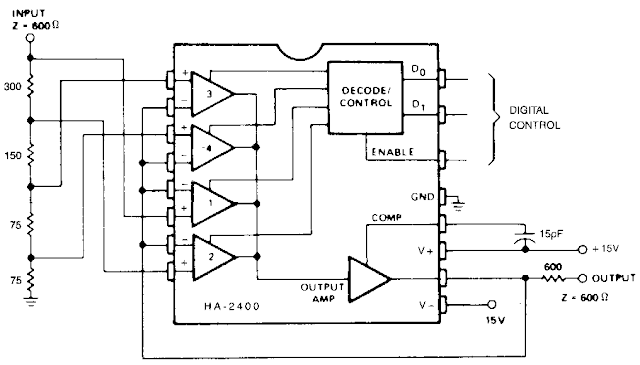
Simple Programmable Attenuator Circuit

This Simple Programmable Attenuator Circuit performs the function of dividing the input signal by a selected constant (1, 2, 4, 8, etc.). While T, Z, or L sections could be used in the input attenuator, this is not necessary since the amplifier loading is negligible and a constant input impedance is maintained. The circuit is thus much simpler and more accurate than the usual method of constructing a constant impedance ladder, and switching sections in and out with analog switches. Two identical circuits can be used to attenuate a balanced line .

Simple Programmable Attenuator Circuit

Simple Programmable Attenuator Circuit

Read More..

Wednesday, July 31, 2013

Simple Small Portable Alarm Circuit

The system of using this circuit is positioning a little magnet close to the stalk switch SW1 while being connected to the hand or garments of the individual holding the sack with the use of a tiny cable. Since the circuit is tiny, it can be put in a tiny plastic box. The magnetic field will definitely loose its contact with the splint change the moment the bag is snatched instantly. The circuit will definitely start oscillating if SW1 starts and will certainly produce a loud alarm sound from the loudspeaker. Alternatively, the unit can be placed in a pocket while the cable is linked to the bag, to develop a reverse approach of connection.

The high efficiency oscillator is made up by electrical wiring a corresponding transistor-pair that will definitely drive a small 8 Ohm loudspeaker directly. A very compact assembly is the result of 3 V electric battery quantity B1 and reasonable count of parts made use of.

Any kind of loudspeaker can be made use of yet the measurement is directed by the box where it will be positioned. Considering that the standby current being drawn is less than 20 uA, it is not required to include an ON/OFF switch. A existing of around ONE HUNDRED mA is consumed by the circuit when the alarm system is sounding. To make the circuit a lot more appealing, a 3.5 mm mono jack can be made use of as substitute for the switch while a 3.55 mm mono jack plug with its interior leads shorted can be made use of in place of the magnet. The tiny cable will certainly be connected to the jack plug. The voltage used to provide this circuit should not go over 4.5 V since the transistor Q2 could acquire ruined. To be on the risk-free side, it is suggested to utilize a 3 V supply with two AA cells wired in series.

The personal alerts are one of the fastest growing portions in the self protection sector today because they are exceptionally loud as well as beneficial to hold. It could be available in the kind of essential chains, rich torches, levered hook, or hand band. It is utilized for scaring off an attacker by unexpected them with high pitch alarm that may attract attention of others in the spot. The opening of a window or doorway may give a signaling procedure utilizing this gadget which can be done by putting the box on the frame as well as the magnetic field on the transferable part. In this way, the splint switch as well as the magnetic field will definitely be extremely close when the window or doorway is closed.
  • BC547 isNPN tiny signal transistors produced for basic application changing and boosting due to its reasonable voltage, low current as well as 3 different gain options
  • BC327 is a PNP basic purpose transistor in a TO-92 bundle, made use of for basic purpose changing and amp applications which is suitable for AF driver periods and inexpensive power outcome stages of audio amps due to its attributes of high current at FIVE HUNDRED mA maximum and inexpensive voltage at 45 V optimum
Read More..

Thursday, July 11, 2013

Simple Ignition Timer Schematic

This circuit is a tester for flywheel based ignition systems in small aeroplane engines. Basically the same ignition coils are also seen in other small combustion engines used in/on mopeds and lawn mowers  in brief, engines without a battery. The part to be tested comprises a primary coil in parallel with the contact breaker. The timing of this contact breaker has to be adjusted correctly.
Since the coil’s primary has a very low resistance it is difficult to determine whether the contact breaker is open or closed.  However, you can determine that reliably with this circuit, using an LED and a beeper. The circuit is implemented twice because aviation engines (Cessna, Piper and similar) always have two ignitions in parallel to increase reliability. For two-cylinder engines, well the purpose is obvious.
Ignition Timer Circuit Diagram
The circuit consists of a 555 and a few transistors. The 555 supplies a square wave of about 3000 Hz. This signal goes to power transistors T1 and T2; these can supply quite a bit of power and are robust enough to withstand the voltage transients from the big coils. The test connection (K2 and K3 respectively) are connected in parallel with the contact breaker to be tested, which itself is in parallel with the ignition coil. The frequency of 3000 Hz is either short circuited by the contact breaker or if the points are open  is amplified somewhat by the resonance of the coil itself.

This allows you to reliably detect the difference bet ween a closed and open contact breaker, despite the low resistance of the coil, which is in parallel with it. When the contact breaker is open the amplified pulses will turn on T3 and T4 respectively, so that the relevant LEDs turn on and the buzzer will sound.

The components are not critical, but do use a sensitive type for the piezo buzzer. The power supply is 3 V (2 times AA or AAA batteries). Link
Read More..

Wednesday, July 10, 2013

Simple HiFi Expandor Circuit Diagram with De emphasis

This is the schematic design of HiFi Expandor Circuit with De-emphasis. The circuit is based NE570. The NE570 can be used to construct a high performance compandor suitable for use with music. This type of system can be used for noise reduction in tape recorders, transmission systems, bucket brigade delay lines, and digital audio systems. The circuits to be described contain features which improve performance, but are not required for all applications.

 HiFi Expandor Circuit  Diagram 
HiFi Expandor Circuit  Diagram

The expandor to complement the compressor is shown in the above circuit. Here an external op amp is used for high slew rate. Both the compressor and expandor have unity gain levels of 0dB. Trim networks are shown for distortion (THD) and DC shift. The distortion trim should be done first, with an input of 0dB at 10kHz. The DC shift should be adjusted for minimum envelope bounce with tone bursts. When applied to consumer tape recorders, the subjective performance of this system is excellent.
Read More..

Tuesday, July 9, 2013

Simple OBD Vehicle Protection

vehicle immobilisers are fitted as standard to modern cars and heavy goods vehicles. Anti-theft mechanisms have become more sophisticated but so have the methods employed by crooks. Nowadays once the thief has gained access to a vehicle they will most likely use an electronic deactivation tool which seeks to disable the immobiliser, once this has been accomplished a blank transponder key/card can be used to start the engine. In many cases communication with the immobiliser is made using the OBD-II diagnostic connector.

Although the OBD-II protocol itself does not support the immobiliser, the vehicle manufacturer is free to use the interface as neces-sary for communication, either the standard OBD-II signals or unused pins in the OBD-II connector (i.e. those undefined in the OBD-II standard). Using one of these pathways the immobiliser can usually be electronically disabled. 

OBD Vehicle Protection Circuit Diagram
OBD-Vehicle-Protection-Circuit Diagram
This may be unsettling news for owners of expensive vehicles but when professional car-thieves call, armed with the latest OBD-II hacking equipment this simple low-cost low-tech solution may be all that you need. The idea is ver y simple: if all connections to the OBD-II connector are disconnected there is no possibility for any equipment, no matter how sophisticated to gain access via the vehicle’s wiring. 

The OBD-II connector is usually locate d underneath the dashboard on the passenger side; once its wiring loom has been identified a switch can be inserted in line with the wires. The switch should be hidden away some-where that is not obvious. In normal opera-tion you will be protected if the vehicle is run with the wires to the socket disconnected. Make sure however that you throw the switch reconnecting the socket before you next take the vehicle along to a garage for servicing or fault diagnosis. 

The diagram shows the ISO K and ISO L wires switched. To cover all bases it is wise for every wire to the socket is made switchable except the two earth connections on pins 4 and 5 and the supply voltage on pin 16. Almost ever y vehicle manufacturer has their own method of vehicle immobilisation, by disconnecting every wire it ensures that no communication is possible (even over the CAN bus). Now the innermost workings of your vehicle will be safe from prying eyes. When a hacker plugs in a deactivation tool it will power up as normal but probably report something like ‘protocol unrecognised’ when any communication with the OBD port is attempted. 


Author : Florian Schäffer - Copyright: Elektor
Read More..

Saturday, July 6, 2013

Simple Mini Bench Supply

Every electronics engineer is familiar with the anxiety of the moment when power is first applied to a newly-built circuit, wondering whether hours of work are about to be destroyed in a puff of smoke. A high-quality power supply with an adjustable current limit function is an excellent aid to steadying the nerves. Unfortunately power supplies with good regulation performance are expensive and homebrew construction is not always straightforward. Many of the ‘laboratory power supplies’ currently on the market are low-cost units based on switching regulators which, although certainly capable of delivering high currents, have rather poor ripple performance. Large output capacitors (which, in the case of a fault, will discharge into your circuit) and voltage over-shoot are other problems.

The power supply described here is a simple unit, easily constructed from standard components. It is only suitable for small loads but otherwise has all the characteristics of its bigger brethren. Between 18 V and 24 V is applied to the input, for example from a laptop power supply. This avoids the need for an expensive transformer and accompanying smoothing. No negative supply is needed, but the output voltage is nevertheless adjustable down to 0 V.  

A difficulty in the design of power supplies with current limiting is the shunt resistor needed to measure the output current, normally connected to a differential amplifier. Frequently in simple designs the amplifier is not powered from a regulated supply, which can lead to an unstable current regulation loop. This circuit avoids the difficulty by using a low-cost fixed voltage regulator to supply the feedback circuit with a stable voltage. This arrangement greatly simplifies current measurement and regulation. 

Mini Bench Supply Circuit Diagram
Mini Bench-Supply-Circuit Diagram
To generate this intermediate supply volt-age we use an LM7815. Its output passes through R17, which measures the output current, to MOSFET T1 which is driven by the voltage regulation opamp IC1C. Here R11 and C4 determine the bandwidth of the control loop, preventing oscillation at high frequencies. R15 ensures that capacitive loads with low effective resistance do not make the control loop unstable.

 The negative feedback of AC components of the current via R12 and C5 makes the circuit reliable even with a large capacitor at its output, and negative feedback of the DC component is via the low-pass filter formed by R14 and C6. This ensures that the volt-age drop across R15 is correctly compensated for. C7 at the output provides a low impedance source for high-frequency loads, and R16 provides for the discharge of C17 when the set voltage is reduced with no load attached. 

Current regulation is carried out by IC1D. Again to ensure stability, the bandwidth of the feedback loop is restricted by R19 and C8. If the voltage dropped across R17 exceeds the value set by P2, the current limit function comes into action and T2 begins to conduct. This in turn reduces the input voltage to the voltage regulation circuit until the desired current is reached. R7, R9 and C3 ensure that current regulation does not lead to output voltage over-shoots and that resonance does not occur with inductive loads. 

The controls of the power supply are all voltage-based. This means, for example¸ that P1 and P2 can be replaced by digital-to-analogue converters or digital potentiometers so that the whole unit can be driven by a microcontroller. IC1B acts as a buffer to ensure that the dynamic characteristics of the circuit are not affected by the setting of P1. IC1A is used as a comparator whose out-put is used to drive two LEDs that indicate whether the supply is in voltage regulation or current regulation mode. If D2 lights the supply is in constant voltage mode; if D1 lights it is in constant current mode, for example if the output has been short-circuited. The power supply thus boasts all the features of a top-class bench supply.IC1A and its surrounding circuitry can be dispensed with if the mode indication is not wanted. 

A type LM324 operational amplifier is suggested as, in contrast to many other similar devices, it operates reliably with input voltages down to 0 V. Other rail-to-rail opamps could equally well be used. The particular n-channel MOSFET devices used are not critical: a BUZ21, IRF540, IRF542 or 2SK1428 could be used for T1, for example, and a BS170 could be used in place of the 2N7002. The capacitors should all be rated for a voltage of 35 V or higher, and R15 and R17 must be at least 0.5 W types. The fixed voltage regulator and T1 must both be equipped with an adequate heatsink. If they are mounted on the same heatsink, they must be isolated from it as the tabs of the two devices are at different potentials. 


Author : Alexander Mumm - Copyright : Elektor
Read More..

Friday, July 5, 2013

Simple SWR and PWR Meter

Many SWR / Power meter used by amateurs to the extent reasonably accurate continuous average power with a CW key-down signal, but can not reliably be used with other (modulated) signals PEP or average power measurement. These laws seek to show why the power measurement can be a sensitive issue, and because the interpretation of a yardstick of power can be a lot of attention and knowledge of construction and the characteristics of the instrument.

A reflectometer-type SWR meter can be calibrated to give power back and forth (PF, Pr) on a power supply. A classic example is the 1943 Bird Series power meter, which is a directional coupler is used to obtain a sample voltage proportional to the voltage wave or forward or backward on the feeder (VF, VR). Other systems, perhaps more suitable for HF, then use a bridge circuit to perform the same function.

 Simple SWR and PWR Meter Circuit diagram 


The sample voltage is then rectified and displayed on a meter that is calibrated in watts. If the counter is typically a coil, the scale, so the numbers on the scale, representing the power, are proportional to the square of the applied voltage or the current calibration. The theory of this type is very simple and is based on the concept represented by PF = Vf2/Zo. Note that if the power supply has an impedance that differs from the value of how the instrument is calibrated, there will be a mistake. The output voltage of the rectifier is a solid phase of VF or VR, and this is expected in the calibration of the meter.

Examples of directional coupling, and bridge-type reflectometers are shown in Figures 1 and 2, while the bird directional coupler means 43 is illustrated in Figure 3. Note that in all cases the measurement circuit, a combination with a small RC time constant, making the system unsuitable for the measurement of PEP, and the absence of a specific device quadratic, making them unsuitable for measuring the average power .
Read More..

Wednesday, July 3, 2013

Simple Fluorescent Light Wiring Diagram Tube Light Circuit

The wiring process of fluorescent tube lamp/light with Ballast,Starter is quite easy and simple. In most cases when we buy a fluorescent light it comes in a complete set with all wire connected. If you want do it yourself , you can buy all the parts individually. And you can complete all connection of the fluorescent light/lamp with the help of this wiring circuit diagram.


Main parts of Fluorescent Tube Light:

     1.Fluorescent Tube
     2.Ballast
     3.Starter
     4.Holder, wire etc.

How Fluorescent Lights works:

The starter is like a key of fluorescent light because it is used to light up the tube. When we connect the AC supply voltage to the circuit, then the starter act like short circuited and current flow through those filament (located at the first and second end of the tube light) and the filament generate heat and it ionized the gas (mercury vapor) in the fluorescent tube lamp. So the gas becomes electrically conductive medium. At the same time when the starter opened the circuit path of two filaments from series connected, then the ballast release its stored voltage. And it makes the fluorescent tube fully lighten. Now the starter has no job in the circuit, if you open it from the circuit the fluorescent tube light will be still lighten, until you release the main supply.
Read More..

Friday, May 31, 2013

Simple Electrical Projects

Basic Electrical Wiring on Simple Electrical Projects
Simple Electrical Projects.


Basic Electrical Wiring on The Damaging Effects Of Electropollution
The Damaging Effects Of Electropollution.


Basic Electrical Wiring on Basic 2 Way Switch Wiring Diagram
Basic 2 Way Switch Wiring Diagram.


Basic Electrical Wiring on How To Install Electrical Wiring   Doityourself Com
How To Install Electrical Wiring Doityourself Com.


Basic Electrical Wiring on Here Iswhat The Electrical Wiring Would Look Like For This Situation
Here Iswhat The Electrical Wiring Would Look Like For This Situation.


Basic Electrical Wiring on Gfci Outlet Wiring Diagram   Pdf  55kb
Gfci Outlet Wiring Diagram Pdf 55kb.


Basic Electrical Wiring on Basic Electrical Connections
Basic Electrical Connections.


Basic Electrical Wiring on Basic Electrical Wiring   Basic Electrical Wiring Project Beginner
Basic Electrical Wiring Basic Electrical Wiring Project Beginner.


Basic Electrical Wiring on Chapter 2   Automotive Electrical Circuits And Wiring
Chapter 2 Automotive Electrical Circuits And Wiring.


Basic Electrical Wiring on Heres A Diagram I Found I Dont Know If Its Helpful Or Not
Heres A Diagram I Found I Dont Know If Its Helpful Or Not.


Read More..

Wednesday, May 29, 2013

Simple 2 1 Surround Speaker System Circuit Diagram

 "Simple 2.1 Surround Speaker System " . Here I have used  three TDA 2030 IC for making signal amplification . Here you need a sub filter extra ( Sub filter circuit diagram link showing below ) . This project  mostly used in computer  . Part list and applications are showing below.

Part List

Component No:ValueUsage
All C1100MF Grounding 
All C2100nFGrounding
All C3100nFGrounding
All C4100MFGrounding
All C5100MFFeedback
All C6100MFAudio Coupling 
All C7220nFNoise Grounding 
All R11K
All R210K ( Not 1K )
All R322K
All R422K (Not 1K )
All RV1100KVolume Controlling 
All D1 To D2IN4007Potential Breaking
U1 To U6TDA2030Amplification

Applications

* 2.1 Surround Amplifier

* 2.1 Home Theater
Read More..

Friday, April 12, 2013

Simple Audio Graphic Equaliser

Audio photograph equalizers are quite common as business products (for Hi-fi, automobile audio and stage use) but circuits for them are very hardly ever printed. I didnt design this one nevertheless its in reality very straightforward. The important levels shown are for a 7 band but the theory will also be prolonged to almost any choice of bands - in case you can in finding correct enough elements. 


\"Audio

Only one gyrator stage is shown: all 7 gyrators are the identical circuit, best the capacitors change, as proven in the chart. I even have shown three of the seven faders to level out where they go. 

A gyrator is a circuit the utilization of active tools and transistors to simulate an inductor. In this case the gyrator is the transistor appearing with R1, R3 and C2. It may just as simply be a cohesion acquire op-amp. 

The circuit embraces three formulae: one which offers f, the the centre frequency of the band. The 2nd shows how the Q is related to the capacitor ratio. The third presentations the impedance offered with the help of the circuit. Note that this embraces 3 time periods, the primary merely resistive, the 2d is the capacitative contribution from C1 and the 0.33 is an inductive term from the gyrator. 

If anyone wants the distinct mathematical working out of these formulae, I could be triggered to submit it (donations accepted!). The arithmetic for energetic filters shouldn't be as tough as most tutors tend to make it and I in point of fact didnt take into account it correctly until I labored it out for myself and found that it wasnt complicated, I simply hadnt been taught how you can take into account it! 

If you do the arithmetics for this you'll in finding the actual frequencies are if truth be told a little completely different from the target frequencies proven within the diagram: thats what comes from the utilization of standard values. Audibly they're masses close enough. 

The rest of the circuit is simply an op-amp. If you imagine a tuned circuit (the gyrator) striking from the pot slider, it's being linked either to the certain input or the poor to a variable extent. One will elevate the response at the turned frequency and the opposite will decrease it. 

You must after all selected a excellent, low noise op-amp: once we manufactured these we used 741s but we chosen low noise ones. The transistors also need to be low noise, however you might easily exchange a noisy transistor in the adventure you to find you will have one. 

And thats about it. A very straightforward, effective circuit. The most tough bit is going to be sourcing the parts - specifically appropriate fader pots!.
Read More..

Simple Universal PIC Programmer

This simple programmer will accept any device thats supported by software (eg, IC-Prog 1.05 by Bonny Gijzen at www.ic-prog.com). The circuit is based in part on the ISP header described in the SILICON CHIP "PIC Testbed" project but also features an external programming voltage supply for laptops and for other situations where the voltage present on the RS232 port is insufficient. This is done using 3-terminal regulators REG1 & REG2. The PIC to be programmed can be mounted on a protoboard. This makes complex socket wiring to support multiple devices unnecessary. 16F84A, 12C509, 16C765 and other devices have all been used successfully with this device.

Circuit diagram:
Simple universal-pic-programmer-circuit-diagramw
Simple Universal PIC Programmer Circuit Diagram


http://www.ecircuitslab.com
Read More..

Thursday, April 11, 2013

Simple Transformerless 5 Volt Power Supply

Description

An increasing number of appliances draw a very small current from the power supply. If you need to design a mains powered device, you could generally choose between a linear and a switch-mode power supply. However, what if the appliance’s total power consumption is very small? Transformer-based power supplies are bulky, while the switchers are generally made to provide greater current output, with a significant increase in complexity, problems involving PCB layout and, inherently, reduced reliability. 

Is it possible to create a simple, minimum part-count mains (230 VAC primary) power supply, without transformers or coils, capable of delivering about 100 mA at, say, 5 V A general approach could be to employ a highly inefficient stabilizer that would rectify AC and, utilizing a zener diode to provide a 5.1 V output, dissipate all the excess from 5.1 V to (230×v2) volts in a resistor. Even if the load would require only about 10 mA, the loss would be approximately 3 watts, so a significant heat dissipation would occur even for such a small power consumption. 

At 100 mA, the useless dissipation would go over 30 W, making this scheme completely unacceptable. Power conversion efficiency is not a major consideration here; instead, the basic problem is how to reduce heavy dissipation and protect the components from burning out. The circuit shown here is one of the simplest ways to achieve the above goals in practice. A JVR varistor is used for overvoltage/surge protection. Voltage divider R1-R2 follows the rectified 230 V and, when it is high enough, T1 turns on and T3 cannot conduct.

Circuit diagram:


When the rectified voltage drops, T1 turns off and T3 starts to conduct current into the reservoir capacitor C1. The interception point (the moment when T1 turns off) is set by P1 (usually set to about 3k3), which controls the total output current capacity of the power supply: reducing P1 makes T1 react later, stopping T3 later, so more current is supplied, but with increased heat dissipation. Components T2, R3 and C2 form a typical ‘soft start’ circuit to reduce current spikes this is necessary in order to limit C1’s charging current when the power supply is initially turned on. At a given setting of P1, the output current through R5 is constant. 

Thus, load R4 takes as much current as it requires, while the rest goes through a zener diode, D5. Knowing the maximum current drawn by the load allows adjusting P1 to such a value as to provide a total current through R5 just 5 to 6 mA over the maximum required by the load. In this way, unnecessary dissipation is much reduced, with zener stabilization function preserved. Zener diode D5 also protects C1 from over voltages, thus enabling te use of low-cost 16 V electrolytics. 

The current flow through R5 and D5, even when the load is disconnected, prevents T3’s gate-source voltage from rising too much and causing damage to device. In addition, T1 need not be a high-voltage transistor, but its current gain should exceed 120 (e.g. BC546B, or even BC547C can be used).

CAUTION!

The circuit is not galvanically isolated from the mains. Touching any part of the circuit (or any circuitry it supplies power to) while in operation, is dangerous and can result in an electric shock! This circuit should not be built or used by individuals without proper knowledge of mains voltage procedures.


Copyright: Elektor Electronics Magazine
Author: Srdjan Jankovic & Branko Milovanovic
Read More..

Monday, April 1, 2013

Simple Stereo VU Meter

I like to see lights move to music. This project will indicate the volume level of the audio going to your speakers by lighting up LEDS. The LEDS can be any color so mix them up and really make it look good. The input of the circuit is connected to the speaker output of your audio amplifier. You want to build two identical units to indicate both right and left channels. The input signal level is adjusted by the 10k ohm VR. If you wish to make a very large scale model of this unit and hang it on your wall there is an optional output transistor that can drive many LEDS at once. The unit I built drove three LEDS for each output. The sequence of the LEDS lighting are as follows Pin 1, 18, 17, 16, 15, 14, 13, 12, 11, 10.


Read More..

Sunday, March 31, 2013

Simple Door Alarm

Hangs up on the door-handle Beeps when someone touches the door-handle from outside

This circuit emits a beep and/or illuminates a LED when someone touches the door-handle from the outside. The alarm will sound until the circuit will be switched-off.  The entire circuit is enclosed in a small plastic or wooden box and should be hanged-up to the door-handle by means of a thick wire hook protruding from the top of the case.
 
A wide-range sensitivity control allows the use of the Door Alarm over a wide variety of door types, handles and locks. The device has proven reliable even when part of the lock comes in contact with the wall (bricks, stones, reinforced concrete), but does not work with all-metal doors. The LED is very useful during setup.


Door Alarm Circuit diagram:
Door Alarm Circuit diagram 
Parts:
R1______________1M   1/4W Resistor
R2______________3K3 1 or 2W Resistor (See Notes)
R3_____________10K 1/2W Trimmer Cermet (See Notes)
R4_____________33K 1/4W Resistor
R5____________150K 1/4W Resistor
R6______________2K2 1/4W Resistor
R7_____________22K 1/4W Resistor
R8______________4K7 1/4W Resistor

C1,C2__________10nF 63V Ceramic or Polyester Capacitors
C3_____________10pF 63V Ceramic Capacitor
C4,C6_________100nF 63V Ceramic or Polyester Capacitors
C5______________2µ2 25V Electrolytic Capacitor
C7____________100µF 25V Electrolytic Capacitor


D1,D2,D4_____1N4148   75V 150mA Diodes
D3_____________5 or 3mm. Red LED

Q1,Q2,Q3,Q5___BC547 45V 100mA NPN Transistors
Q4____________BC557 45V 100mA PNP Transistor

L1_________________ (See Notes)
L2_____________10mH miniature Inductor

Hook_______________ (See Notes)

BZ1___________Piezo sounder (incorporating 3KHz oscillator)

SW1,SW2________SPST miniature Slider Switches

B1_______________9V PP3 Battery

Clip for PP3 Battery


Circuit operation:

Q1 forms a free-running oscillator: its output bursts drive Q2 into saturation, so Q3 and the LED are off. When part of a human body comes in contact with a metal handle electrically connected to the wire hook, the body capacitance damps Q1 oscillations, Q2 biasing falls off and the transistor becomes non conducting. Therefore, current can flow into Q3 base and D3 illuminates. If SW1 is closed, a self-latching circuit formed by Q4 & Q5 is triggered and the beeper BZ1 is activated.

When the human body part leaves the handle, the LED switches-off but the beeper continues to sound, due to the self-latching behavior of Q4 & Q5. To stop the beeper action, the entire circuit must be switched-off opening SW2. R3 is the sensitivity control, allowing to cope with a wide variety of door types, handles and locks.

Notes:
  • L1 is formed winding 20 to 30 turns of 0.4mm. diameter enameled copper wire on R2 body and soldering the coil ends to the resistor leads. You should fill R2 body completely with coil winding: the final turns number can vary slightly, depending on different 1 or 2W resistor types actual length (mean dimensions for these components are 13 - 18mm. length and 5 - 6mm. diameter).
  • The hook is made from non-insulated wire 1 - 2mm. diameter (brass is well suited). Its length can vary from about 5 to 10cm. (not critical).
  • If the device is moved frequently to different doors, Trimmer R3 can be substituted by a common linear potentiometer fitted with outer knob for easy setup.
  • To setup the device hang-up the hook to the door-handle (with the door closed), open SW1 and switch-on the circuit. Adjust R3 until the LED illuminates, then turn slowly backwards the screwdriver (or the knob) until the LED is completely off. At this point, touching the door-handle with your hand the LED should illuminate, going off when the hand is withdrawn. Finally, close SW1 and the beeper will sound when the door-handle will be touched again, but will not stop until SW2 is opened.
  • In regular use, it is advisable to hang-up and power-on the device with SW1 open: when all is well settled, SW1 can be closed. This precautionary measure is necessary to avoid unwanted triggering of the beeper.
Source : http://www.ecircuitslab.com/2011/06/door-alarm-circuit.html
Read More..

Thursday, March 28, 2013

Simple Video Amplifier

The video amplifier in the diagram is a well-known design. Simple, yet very useful, were it not for the ease with which the transistors can be damaged if the potentiometers (black level and signal amplitude) are in their extreme position. Fortunately, this can be obviated by the addition of two resistors. If in the diagram R3 and R4 were direct connections, as in the original design, and P1 were fully clockwise and P2 fully anticlockwise, such a large base current would flow through T1 that this transistor would give up the ghost.

 Video Amplifier Circuit diagram :


Moreover, with the wiper of P2 at earth level, the base current of T2 would be dangerously high. Resistors R3 and R4 are sufficient protection against such mishaps, since they limit the base currents to a level of not more than 5 mA. Shunt capacitor C4 prevents R4 having an adverse effect on the amplification.

Source :   http://www.ecircuitslab.com/2011/06/video-amplifier-circuit-diagram.html
Read More..

Wednesday, March 27, 2013

Simple 9 Way Cable Identifier

Here is a simple way of identifying multiple cables (with the aid of a multimeter). The circuit consists of a series of resistors, selected so that they give readings that coincide with the 1-9 numerals on the 10V scale on a multimeter switched to the Ohms x 100 range. In use, a common wire needs to be chosen and this is usually the shield wire.

The resistors go to one end of the cables to be identified, while the multimeter is used at the other end to check the values and identify each lead. Up to nine cables can be identified at a time. If a mistake is made in choosing the common lead, the readings will all be wide of the 1-9 numerals on the 10V scale, thus making the mis­take obvious.

Circuit diagram:

simple-9-way-cable-identifier-circuit-diagram1 Simple 9-Way Cable Identifier

Source : http://www.extremecircuits.net

Read More..