Wednesday, December 18, 2013
Build a high volt supply Circuit Diagram

Friday, October 4, 2013
Mini High Voltage Generator Circuit
Here’s a project that could be useful this summer on the beach, to stop anyone touching your things left on your beach towel while you’ve gone swimming; you might equally well use it at the office or workshop when you go back to work. In a very small space, and powered by simple primary cells or rechargeable batteries, the proposed circuit generates a low-energy, high voltage of the order of around 200 to 400 V, harmless to humans, of course, but still able to give a quite nasty ‘poke’ to anyone who touches it.
Quite apart from this practical aspect, this project will also prove instructional for younger hobbyists, enabling them to discover a circuit that all the ‘oldies’ who’ve worked in radio, and having enjoyed valve technology in particular, are bound to be familiar with. As the circuit diagram shows, the project is extremely simple, as it contains only a single active element, and then it’s only a fairly ordinary transistor. As shown here, it operates as a low-frequency oscillator, making it possible to convert the battery’s DC voltage into an AC voltage that can be stepped up via the transformer.
Using a centre-tapped transformer as here makes it possible to build a ‘Hartley’ oscillator around transistor T1, which as we have indicated above was used a great deal in radio in that distant era when valves reigned supreme and these was no sign of silicon taking over and turning most electronics into ‘solid state’. The ‘Hartley’ is one of a number of L-C oscillator designs that made it to eternal fame and was named after its invertor, Ralph V.L Hartley (1888-1970). For such an oscillator to work and produce a proper sinewave output, the position of the intermediate tap on the winding used had to be carefully chosen to ensure the proper step-down (voltage reduction) ratio.
Here the step-down is obtained inductively. Here, optimum inductive tapping is not possible since we are using a standard, off-the-shelf transformer. However we’re in luck — as its position in the centre of the winding creates too much feedback, it ensures that the oscillator will always start reliably. However, the excess feedback means that it doesn’t generate sinewaves; indeed, far from it. But that’s not important for this sort of application, and the transformer copes very well with it.
The output voltage may be used directly, via the two current-limiting resistors R2 an R3, which must not under any circum-stances be omitted or modified, as they are what make the circuit safe. You will then get around 200 V peak-to-peak, which is already quite unpleasant to touch. But you can also use a voltage doubler, shown at the bottom right of the figure, which will then produce around 300 V, even more unpleasant to touch. Here too of course, the resistors, now know as R4 and R5, must always be present. The circuit only consumes around a few tens of mA, regardless of whether it is ‘warding off’ someone or not! If you have to use it for long periods, we would however recommend powering it from AAA size Ni-MH batteries in groups of ten in a suitable holder, in order not to ruin you buying dry batteries.
Circuit diagram:

Warning!
If you build the version without the voltage doubler and measure the output voltage with your multimeter, you’ll see a lower value than stated. This is due to the fact that the waveform is a long way from being a sinewave, and multimeters have trouble interpreting its RMS (root-mean-square) value. However, if you have access to an oscilloscope capable of handling a few hundred volts on its input, you’ll be able to see the true values as stated. If you’re still not convinced, all you need do is touch the output terminals...
To use this project to protect the handle of your beach bag or your attachecase, for example, all you need do is fix to this two small metallic areas, quite close together, each connected to one output terminal of the circuit. Arrange them in such a way that unwanted hands are bound to touch both of them together; the result is guaranteed! Just take care to avoid getting caught in your own trap when you take your bag to turn the circuit off!
Copyright : Elektor Electronics 2008
Thursday, July 11, 2013
High intensity LED Warning Flasher Circuit Diagram

The flash frequency is about one per second and the LED on-time is about 330 ms. The duty cycle should enable the batteries to power the circuit over night. The circuit is composed of three parts. Under normal daylight conditions the batteries are charged through diode D4. In darkness, pnp transistor T1 is switched on, supplying battery current to the second part, a low-frequency oscillator comprising T2 and T3.The third part is the LED driver around T4.
It conducts and switches on the LEDs D1-D2-D3 when the collector voltage of T3 swings high. Two LEDs (D1, D2) are 20,000-30,000 mcd high-brightness yellow types and one (D3) is a normal 3-mm red LED for control purposes. Of course it is possible to increase the number of LEDs to obtain higher brightness. However you will run into limitations regarding the maximum collector current of transistor T4. For really high power applications a MOSFET transistor is suggested instead of the common or garden BC547B.
Tuesday, July 9, 2013
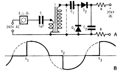
12KV High Voltage Generator

Wednesday, July 3, 2013
Dual High Side Switch Controller
Circuit diagram :

Wednesday, April 10, 2013
High Input Voltage Linear Regulator
 This 1.20V is amplified by the external resistor ratio of R1 and R2. An internal constant bias current of 10µA is connected to the ADJ pin so that Vout is increased by a constant voltage of 10µA times R2. The formula for calculating the output voltage is given next to the circuit diagram. To ensure stable operation of the regulator a minimum output current of 500µA is necessary and a bypass capacitor of minimum 1.0µF should be used. Protection circuits in the LR8 limit the output current to 15mA typically and temperature protection ensures that the device temperature will not exceed 125oC.
 When the device reaches its temperature limit, the output voltage/current will decrease to keep the junction temperature within limits. The two circuit diagrams show the LR8 used as a voltage regulator and as a constant current source. The current source can be used to a drive an LED. This configuration would give an LED with super-wide input voltage range, i.e., from +12V to +450V. The LR8 was originally designed to be used for switch mode supply start-up applications so it incorporates a feature which shuts down the LR8 when the output voltage exceeds the input voltage. Diode D1 is therefore necessary in the voltage regulator circuit diagram to prevent the output voltage exceeding the input voltage at any time.
 The minimum value of the input capacitor C1 can be calculated from the following formula: C1(min) = (IL t ) / (Vpk – Vout – 10V) Where IL is the load current, and t the period between two voltage peaks. At 50 Hz, using one rectifying diode this will give a value t = 20 ms. Vpk is the peak input voltage, while Vout is the selected output voltage. The LR8 is available in two package outlines. The LR8N8 is a SOT89 SMD package while the LR8N3 is the familiar TO92 Transistor outline (e.g. BC 238). The TO-92 package can dissipate a maximum of 0.74W while with suitable heatsinking, the SMD package can dissipate 1.6W.